Phono Preamp Design Using Active RIAA Equalization
Introduction
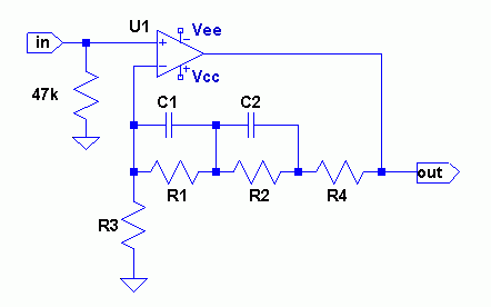
This page contains equations and a procedure for accurately computing the circuit component values for a phono preamp using active RIAA equalization. The circuit to be discussed is shown in Figure 1 below. The equations also apply to the inverse RIAA network often used for bench testing, provided the network has the same topology as the feedback network of Figure 1. This subject has certainly been beaten to death many times over the years, so why should anyone present yet another analysis of the circuit? Lipshitz has already covered this circuit and a number of others in excruciating detail in [1] for example. There are several reasons for this.
Practical Considerations
The analysis in [1] is complex and can be difficult to follow. It takes into account the IEC amendment to the RIAA standard. This introduces two additional time constants at low frequencies, making the formulas more complex than they need to be. The IEC amendment provides for a single low-frequency pole at 20 Hz to reduce rumble and warp effects. Real-world circuits can provide improved performaince in this area by using a separate second- or third-order filter, possibly with a lower cutoff frequency than the 20 Hz value specified by the IEC. Some good information on this subject can be found in this paper by Holman. The IEC extension will be ignored here, since it's assumed you'll want to have the best low-frequency performance possible. Further discussion of the IEC amendment and the controversy surrounding it can be found in Keith Howard's Stereophile article on RIAA equalization [6].
Another concern is the practical constraints that can get in the way of accurate equalization. A good design technique allows the designer to pick the capacitor values, then determine the resistors. That's the approach followed here. This allows for maximum flexibility in the design approach because of the relative shortage of readily obtainable standard capacitor values compared to resistors. When highest accuracy is needed and the designer has very accurate capacitance measurement capability, capacitors could be measured, picked and matched between channels, then resistors calculated and possibly also measured and picked to get as close as possible to calculated values.
The Controversy of the So-Called "Neumann Time Constant"
When I originally wrote this article, I placed emphasis on using the circuit to realize the what's come to be known as the "Neumann time constant". The use of this extra time constant was originally described in an article by Allen Wright [2], and later picked up by Jim Hagerman [3]. In the first linked article, Wright asserted that the equalization curve used by Neumann cutting lathes has additional low-pass filtering not specified by the RIAA curve. He claimed the additional filtering to be a simple pole at approximately 50.05 kHz, corresponding to a time constant value of 3.18 microseconds. This was apparently the origin of the term "Neumann time constant". However, it's been pointed out by people familiar with the design of Neumann cutting lathes that this filtering varies with cutting lathe model, both in the nominal -3 dB frequency and in the number of poles of the filter. It is therefore impossible for the equalization of the phono preamp to compensate for the cutting lathe low-pass characteristics in general. In intervening years, a backlash against the inclusion of the Neumann time constant in phono preamp designs began to develop in the literature. This opposing view is articulated quite well in an article by Keith Howard for Stereophile [6]. Douglas Self's book Small Signal Audio Design [7] also recommends against implementing the Neumann time constant.
That being said, the circuit of Figure 1 unavoidably creates an extra zero in the transfer function, whether it's desired or not. The choice then becomes one of either implementing the so-called Neumann time constant, or choosing the frequency of the zero such that it's high enough to not interfere in a significant way with RIAA equalization accuracy at the high end of the frequency band. It will be shown later in this article that once the frequency of this zero is chosen, the ratio of the two capacitors C1 and C2 in Figure 1 is uniquely determined. Therefore, it's possible to choose the frequency of the zero such that the capacitor ratio corresponds exactly to the ratio of nominal standard capacitor values. More detail of this approach is provided later in this article. The specific example discussed here does use the Neumann time constant to determine the desired frequency of the extra zero, but given the controversial nature of this approach, the example should be treated as being for illustrative purposes only. For additional information on the design of this network for the extra time constant, see Hagerman [3]. He has done an analysis of the circuit of Figure 1 and provided a network whose high-frequency zero matches the 3.18 microsecond time constant specified by Wright. His analysis uses SPICE optimization to get the required component values. The analysis here provides explicit formulas for the required component values and thus allows families of networks to be created.
General Approach
The analysis provided here uses a modern network synthesis approach (Guillemin [4]) to derive simple explicit formulas for each component value individually. This approach is fully described in the appendix. I think you'll find the design equations summarized here to have a simpler form than the analysis of [1].
Before I get too far, I'd like to mention that some people prefer passive RIAA equalization to the active approach, even though it's inferior from the point of view of overload performancs. If that's your view, then this article may not be for you. But even if you don't plan on using active equalization, you may still be interested in designing an inverse RIAA network for your bench testing. The approach described here works for both active RIAA phono preamp design and the design of inverse RIAA networks.
I'll first assume an ideal op-amp. Then we'll look at errors that can be introduced by the finite DC open-loop gain and finite gain-bandwidth product of the op-amp. Since the focus of this procedure is on obtaining high accuracy with real-world components, we'd like an approach that involves first picking the capacitors from the rather small set of available standard values, then picking the resistors to get the desired time constants. I've taken this need into account in the formulas and the procedure. Where necessary, we'll use series or parallel combinations of components to get the precise time constants we're looking for. Also, we'd like to avoid having to use parallel capacitors if possible. However, because of certain constraints of the design that we'll discuss later, this may not always be possible.
Design Equations
The transfer function we want to implement is given by:
| (1) |
where
For convenience, we define:
| (2) | |
| (3) | |
| (4) | |
| (5) |
The time constants T1, T2 and T3 are specified by the RIAA. The value T4 is the extra time constant discussed earlier.
By making the assumption of an ideal op-amp, we reduce the problem to one of finding the R and C values of the feedback network which has a transfer function that's the reciprocal of equation (1). Using passive network synthesis techniques, it's possible to obtain the component values exactly, without resorting to any approximations other than the ideal op-amp assumption. The detailed derivation of these design equations is provided in the appendix. Performing the synthesis procedure results in the formulas below. The component values are expressed in terms of the impedance scale factor RSCALE. The set of all possible networks can be determined by varying RSCALE and k. To obtain the actual component values, C1 and C2 are first chosen, which then determines RSCALE and ω4. Then the remaining component values are computed. The values for the resistors and capacitors are given by:
| (6) |
| (7) |
| (8) |
| (9) |
If we assume R4 = kR3, we obtain:
| (10) |
| (11) |
| (12) |
We can also see that:
| (13) |
and
| (14) |
Finally, we divide equation (9) by equation (7) to obtain:
| (15) |
Design Procedure: Extra Time Constant and the Ideal Capacitor Ratio
We can see that once we pick ω4 by by choosing the extra time constant, all the quantities on the right-hand-side of equation (15) are known. This leads to an important result. The capacitor ratio uniquely determines the extra time constant. Alternatively, the extra time constant uniquely determines the capacitor ratio. I'll assume for purposes of illustration that ω4 is the reciprocal of the so-called Neumann time constant of 3.18 microseconds as previously mentioned. Plugging the numbers in to (15), we obtain this ideal ratio:
| (16a) |
or
| (16b) |
Our design procedure begins by picking C1 and C2. We pick them so their ratio is as close as possible to the ideal ratio given by equations (16). Because the chosen capacitor values won't have the exact ideal ratio, errors will occur. Since ω4 is out of the audio range, we will target ω1, ω2 and ω3 to their ideal values as usual, and absorb the error due to the non-ideal capacitor ratio into an error in ω4. Thus we pick the capacitor ratio C1/C2 and solve for the actual ω4 that results, using equation (15). Once we compute the actual value of ω4, we must use this computed value (rather than the ideal value) in equations (6) through (9) to calculate the resistor values. This is necessary because these equations express the component values in terms of the actual poles and zeros of the network, rather than some ideal target value which we already know we can't meet exactly because of the assumed non-ideal capacitor ratio.
We solve for ω4 in equation (15), resulting in:
| (17) |
Suppose we wish to eliminate the need to have parallel capacitors to achieve the required capacitor ratio given by (15) and instead require that only a total of two capacitors is allowed. We could first pick a nominal value of T4 so that its effect in the audio band is negligible, as was done by Lipshitz. Then we could compute the required capacitor ratio to achieve this from (15). In general, this will not correspond exactly to any ratio of standard capacitor values. Through trial and error, we could find the closest capacitor ratio using standard capacitor values. The resulting resistor values could be checked using (13) and (14) to see if they're reasonable. Once this is done, we could plug that actual capacitor ratio into (17) to find the new value of ω4. If this new value is reasonably close to the desired one, we could then use this adjusted ω4 value to determine the resistors. The result would be a network containing only two capacitors, with resistors chosen to match the desired time constants, possibly using series and/or parallel combinations of resistors. We won't use this approach here. Instead, we'll use the Neumann time constant as an illustrative example.
Before doing the example design, we'd like to know how sensitive ω4 is to the ratio C1/C2. We can compute f4 = ω4 / 2π for the ideal capacitor ratio, then vary the capacitor ratio by, say, 1% to see how much f4 changes. Plugging equation (16) into equation (17) gives f4 = 50.04873 kHz. Increasing C2 by 1% gives f4 = 40.73198 kHz. So a 1% change in the capacitor ratio results in an 18.6% change in f4. We see that f4 is extremely sensitive to the capacitor ratio. This computation assumes that the other poles and zeros stay fixed, which in reality won't be true if only the capacitors are varied. We know from equations (13) and (14) that R1 and R2 must be adjusted for T1 and T3 to remain constant as C1 and C2 vary. However, the situation isn't as uncertain as it might seem. If C1 were changed by 1% and R1 held fixed, then T1 would change by only 1%, T3 would not change at all, and T2 would likely change, but by an unknown (hopefully small) amount. Thus it's prudent to assume that getting the capacitor ratio correct is critical to the accuracy of the network. One mitigating factor is that f4 is outside the audio range, so variations in f4 won't have an extreme effect on the equalization accuracy.
One minor item also remains before we can do the example. Since phono preamps are normally designed for a specific gain at 1 kHz, we need to know the relationship between the 1 kHz gain and the asymptotic low-frequency gain A0. Plugging into equation (1), we find that
So A0 = 9.895779*A(1kHz). Now we're ready to design the network.
Design Example
For this example, we'll choose a low-frequency gain of 54.909 dB, which gives
| (18) |
and a gain at 1 kHz of 35.0 dB. This example is to illustrate making T4 equal to the so-called Neumann time constant, so the target capacitor ratio is determined from equation (16a). We first pick C1 and C2 using a trial and error approach to get as close as possible to this ideal capacitor ratio. Experimentation shows that if we pick
and
we get the capacitor ratio
which gives 0.023% error from the ideal ratio given by equation (16). The actual error will of course be dominated by the capacitor tolerances. Using equation (17), we then compute ω4. The result is:
| (19) |
which is an error of -0.54% from the ideal value computed from the nominal 3.18 microsecond time constant. Given the high sensitivity of ω4 to C2 / C1, this is about as close as can be achieved using standard capacitor values. Again, capacitor tolerances will dominate the actual error. We then compute R1 from equation (13) and R2 from equation (14). The results are:
| (20) |
and
| (21) |
R2 is a standard value and R1 can be implemented as 909k in series with 12.7k. We can now compute RSCALE from any of equations (6), (7), (8) or (9). We get:
| (22) |
We can solve for the resistor ratio k = R4 / R3 from equation (12), giving:
| (23) |
Substituting the numbers, we get:
| (24) |
Plugging in RSCALE and k into equations (10) and (11) we get:
| (25) |
| (26) |
We'd like to avoid using series or parallel combinations of resistors to compensate for the non-standard computed values for R3 and R4. There's a useful tweak that can be performed at this point to help simplify the final circuit. As long as R3 and R4 add up to RSCALE, the equalization accuracy won't be affected at all if we change k. Only the gain is affected. More will be said about this in the appendix. So we can choose R4 = 2.49k and recompute R3. Our final values are:
| (27) | |
| (28) |
Choosing R3 = 1.78k gives a 0.063% error in RSCALE from its ideal value. The final network is shown below without the op-amp
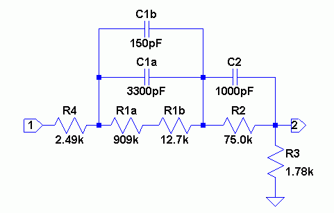
One final note on the circuit before looking at the equalization accuracy. Figure 2 really represents a family of circuits giving different gains. As long as R3 and R4 add up to RSCALE (4267.311 Ohms), only the gain, not any of the time constants, will be affected as we vary the ratio R4/R3. Again, more will be said about this in the appendix. The gain is proportional to (1 + R4/R3) = 1 + k. At 1 kHz, the gain of the circuit when hooked up to an op-amp is 35.08 dB. It's different from the target value of 35.0 dB because we adjusted R4 to a standard value and recomputed R3. To change the gain of the circuit, all that's necessary is to calculate a new value of R4/R3 to get the desired gain, holding RSCALE constant. If the new ratio is knew and the reference ratio is kref, the new gain is Anew and the reference gain Aref, we can compute knew from:
| (29) |
Accuracy of RIAA equalization
There are two categories of circuit design errors that could lead to RIAA equalization accuracy errors.
The first is component value errors. These could be due to component tolerances, the need to pick components from a limited list of standard values, or approximations in the design equations causing the nominal component values to be in error. A full study of component tolerances requires the ability to do Monte Carlo analysis on the circuit. I'll only do a cursory coverage of component tolerance issues here. A full coverage of this issue is, as the old saying goes, beyond the scope of this article. Regarding the accuracy of the design equations, the appendix will show that for an ideal op-amp, these equations are exact and don't depend on any other approximations. You've probably noticed in the design example and its preceding discussion that picking the capacitors first to get as close to the ideal ratio as possible, then picking the resistors will bring benefits to the accuracy of the computed component values. Further, the technique for adjusting R3 and R4 to sacrifice a small amount of gain accuracy in order to improve the time constant accuracy reduces the errors caused by the need for choosing standard resistor values.
The second category of errors is the finite open-loop gain of the op-amp at low frequencies, and the op-amp's finite gain-bandwidth product. The closed-loop voltage transfer function of the circuit of Figure 1 is given by:
| (30) |
where A(s) is the open-loop gain of the op-amp and β(s) is the voltage transfer function of the feedback network. If A(s) is very large, equation (30) reduces to:
| (31) |
This is the only approximation used in the synthesis procedure described here. To get a handle on the errors due to the non-ideal op-amp properties, equation (30) can be rewritten as:
| (32) |
We can then see that the error ε(s) from the ideal transfer function is given by:
| (33) |
Comparing equations (30) and (33) suggests a technique for SPICE that can be used to evaluate the equalization errors due to the non-ideal op-amp. By making a copy of the feedback network, driving this second network from the op-amp output, and taking the test output at the output of the copied feedback network, equation (33) can be simulated directly. This allows direct computation and display of the op-amp-induced errors. A technique for evaluating the total equalization error is also needed. In SPICE, a voltage-controlled voltage source whose scale factor is a LAPLACE expression containing the ideal RIAA time constants and the chosen value of the T4 time constant can be used. By comparing the op-amp output with the output of the LAPLACE controlled source, the total equalization error can be computed. It is then possible to put the op-amp-induced equalization error and the total equalization error on the same graph. If the feedback network were designed perfectly, the two equalization errors would be equal. That is, the total equalization error would be dominated by the op-amp-induced error. This is the result we'd like to achieve. Figure 3 shows a SPICE schematic using these approaches.
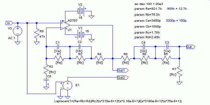
The LAPLACE expression is repeated for clarity below.
Laplace=(1+(Ra+Rb+Rd)/Rc)*(s*318e-6+1)*(s*3.18e-6+1)/((s*3180e-6+1)*(s*75e-6+1))
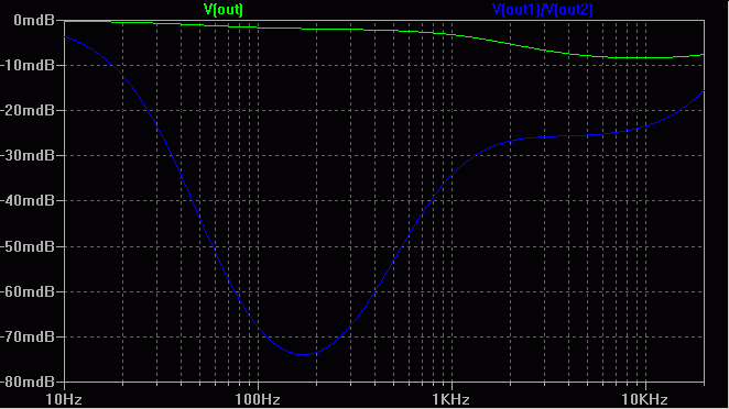
You can see that the exact time constants are plugged into this expression, including the nominal 3.18 microsecond "Neumann" time constant. When choosing a different target value of that time constant, that specific value should of course be plugged into the Laplace expression. The DC value of this expression is equal to what the closed-loop gain of the circuit would be at DC if the op-amp were ideal. Figure 4 below shows the computed errors using an AD797 op-amp.
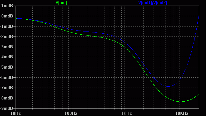
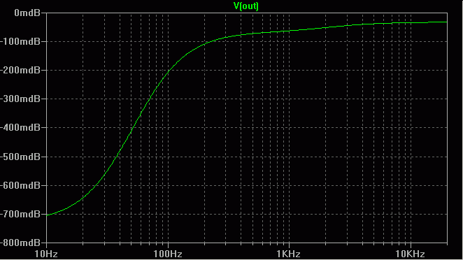
The total equalization error is shown in blue, while the op-amp-induced errors are shown in green. We can see that the errors are mostly dominated by the op-amp-induced errors, except at the highest frequencies. The deviation at high frequencies is due to the -0.54% error we computed in ω4 caused by the small deviation of the capacitor ratio from its ideal value. Since ω4 is slightly lower than its nominal value, we get a slight rise at the high frequencies. It's worth noting that a 0.023% error from the ideal capacitor ratio caused this effect. Let's put this into perspective. The above error looks great on paper (note the 0.001 dB/div scale), but the component value tolerances will blow this out of the water. While I don't intend to do a thorough analysis of the effect of component tolerances on total error, I'll do a simple test in which the value of C1 is increased by 1%. This will give a rough idea of the order of magnitude of the errors that can be expected. The simulated error with C1 increased by 1% is shown below in Figure 5.
It's clear from this change that the component tolerances dominate the error. Notice that the scale is now 0.01 dB/div.
Op-amp guidelines
The subject of "what's the best op-amp for audio use" is a religious issue with many audiophiles. My purpose here is only to briefly demonstrate some effects of non-ideal op-amp behavior on the equalization accuracy of this specific circuit, not recommend any specific one. Two electrical parameters immediately come to mind when considering the equalization accuracy. First, we observe that the low-frequency closed-loop gain of the circuit in this example is quite large - about 55 dB. So we expect the DC open-loop gain to be an important parameter for low-frequency equalization accuracy. Likewise, at high frequencies, the amount of loop gain we get will be determined by the op-amp's gain-bandwidth product. It seems reasonable that for best equalization accuracy, we should choose an op-amp that has a large DC open-loop gain and a large gain-bandwidth product. The AD797, which I've chosen for the purpose of demonstration, has a typical DC open-loop gain of 146 dB and a gain-bandwidth product of about 100 MHz. So we expect good equalization accuracy with this device, and the data confirms this. Now let's look at the effect of reducing the DC open-loop gain. One popular op-amp for audio use is the AD825.
Let's see what kind of equalization error we get with this device. The plot of the op-amp-induced error is shown in Figure 6 below.
We can see that the equalization error is rather large with this device. What happened? The DC open-loop gain of the AD825 is typically 76 dB. Because the target closed-loop gain of our circuit at DC is 55 dB, we don't have enough loop gain at low frequencies. We conclude that the AD825 is not well suited to this application.
Now we'll have a look at the effect of finite DC open-loop gain on equalization accuracy in a more general way. For this simulation, I'll use a generic single-pole op-amp model. I'll make the gain-bandwidth product 1 GHz to minimize high-frequency errors. I'll step the DC open-loop gain from 80 dB to 120 dB in 5 dB steps. Figure 7 shows the op-amp-induced equalization error.
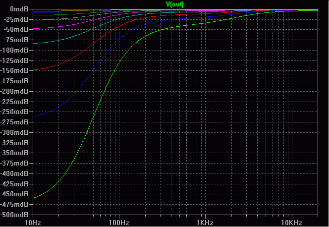
It's seen that the DC open-loop gain must be slightly less than 115 dB to keep the equalization error below 0.01 dB. For a DC open-loop gain of 100 dB, the equalization error is a little less than 0.05 dB.
Next, we'll have a brief look at the effect of finite gain-bandwidth product of the op-amp. This time I'll use a generic single-pole op-amp model with a DC open-loop gain of 160 dB to minimize low-frequency errors. I'll step the gain-bandwidth product from 10 MHz to 100 MHz in 5 MHz steps. Figure 8 shows the op-amp-induced equalization error.
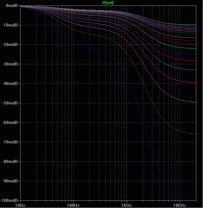
The gain-bandwidth product must be about 100 MHz to keep the op-amp-induced error at 20 kHz from exceeding 0.01 dB. For a 20 MHz gain-bandwidth product, the op-amp-induced error at 20 kHz is close to 0.05 dB.
The Lipshitz paper deals with analytical approaches for computing the component values for the cases of finite DC open-loop gain and finite gain-bandwidth product. I won't attempt to do that here, as it complicates the design process, and some parameters such as the DC open-loop gain may not be well controlled.
References
[1] Lipshitz, On RIAA Equalization Networks, JAES, Vol. 27, June 1979, p. 458-481
[2] Wright, Secrets of the Phono Stage
[3] Hagerman, On Reference RIAA Networks
[4] Guillemin, Synthesis of Passive Networks, John Wiley and Sons: New York, 1957
[5] Weinberg, Network Analysis and Synthesis, Wiley, 1966
[6] Howard, Keith, Cut and Thrust: RIAA LP Equalization, Stereophile, March 2009
[7] Self, Douglas, Small Signal Audio Design, Focal Press